10+ mux block diagram
10 Pictures about block diagram of frequency modulation - Electronics Coach. Intel Stratix 10 MX Devices 12.

Building A Custom Test Multiplexer With No Engineering Required Pulse Research Lab
OC-192 communications system block diagram Laser 10 Gbs Mod TIA Preamp 10 Gbs Photo Diode 10 GHz 16 TX E O Network Processor 622 Mbs 16 O E RX 10.
. Innovations in Intel Stratix 10 MX Devices 13. MUX circuit block diagram is shown in Fig. Logic diagram for for 81 MUX RothKinney Example of MUX application Multiplexers are frequently used to select between two vectors words of data like in.
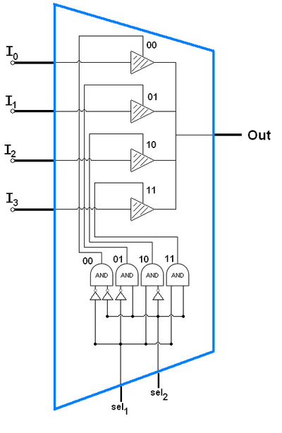
The block diagram of 4x1 Multiplexer is. Electronics Hub - Tech Reviews Guides How-to Latest Trends. It uses a tree architecture with a recursive series of 2.
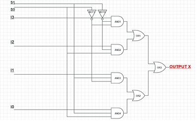
Exploreroots Paralle Adder. In this logic diagram the output is ORed of four ANDed gate. Intel Stratix 10 MX Features Summary 14.
1 multiplexer stages 5. We present an integrated 21 multiplexer and a companion 12 demultiplexer in CMOS. The logical diagram of 4 to 1 MUX is shown below.
Below the given truth table of 4. 22 IO Switch Detection Interface Programmable Wetting Current Analog Mux Block Diagram View additional information for 22 IO MSDI Programmable Current Analog Mux. Adder parallel binary bit circuit carry serial bits.
Which are clearly shown in figure. Unit block diagram control main temperature figure. Intel Stratix 10 MX Block Diagram 15.
4x1 Multiplexer has four data inputs I 3 I 2 I 1 I 0 two selection lines s 1 s 0 and one output Y. 1Draw the block diagram for a 4 to 1 multiplexer circuit. Multiplexer is also called as Mux.
The 21 multiplexer features two in. And write the final equation for inputs and output in both your report and block diagram. Block diagram of frequency modulation - Electronics Coach.
The logic family chosen for this design is emitter- coupled logic. 10 points 2Draw a top-level block diagram. Block diagram of the 21 MUX IC.
Both integrated circuits ICs operate up to a bit rate of 40 Gbs.

Building A Custom Test Multiplexer With No Engineering Required Pulse Research Lab

Multiplexer Wikiwand

Block Diagram Of The Receiver Section All High Speed Signal Download Scientific Diagram
2
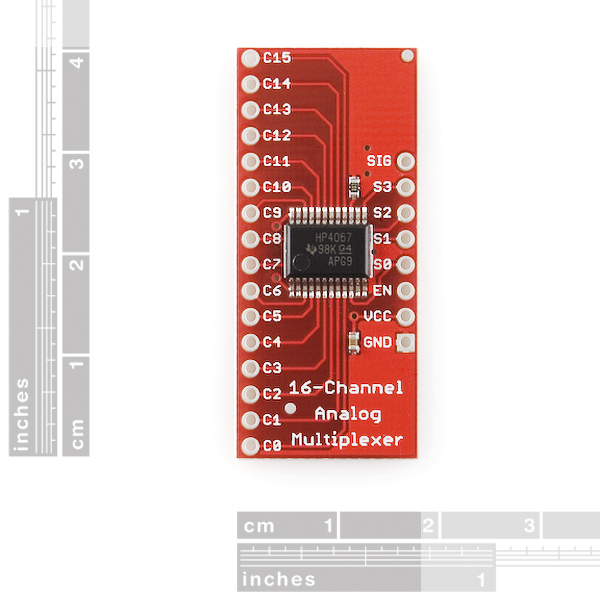
Sparkfun Analog Digital Mux Breakout Cd74hc4067 Bob 09056 Sparkfun Electronics

Building A Custom Test Multiplexer With No Engineering Required Pulse Research Lab
2

Multiplexer Wikiwand
Multiplexer Wikiwand

Block Diagram Of The Receiver Section All High Speed Signal Download Scientific Diagram
Multiplexer Wikiwand
Time Interleaving Springerlink

Implementing A Two Axis Robot Arm Controller Without An Mcu Edn Asia

5 1 1 Ltc6804 1 Based 12 Cell Slave V1 X X Foxbms 2 1 4 0 Documentation

Scaling Capacity Of Fiber Optic Transmission Systems Via Silicon Photonics

Multiplexer Logisim 16 Bit Bits Block Diagram
Encoder Digital Wikiwand